NVIDIA H100 NVL 94GB
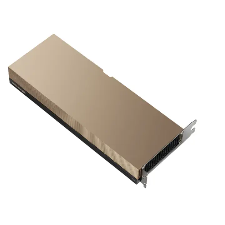
94 GB HBM3 card sold singly but deployed in bridged pairs, at 400 W a card and 188 GB a pair, all three bridges required.
NVIDIA H100 NVL 94GB is one of 24 data center GPUs tracked in the SecondWatt catalogue, each with specifications, lead times and indicative secondary-market pricing.
NVIDIA H100 NVL 94GB specs and power: 400 W passive card, 94 GB HBM3 at 3,938 GB/s, and 188 GB per NVLink-bridged pair requiring all three bridges.
The H100 NVL 94GB is a full-height, full-length dual-slot passive card carrying 94 GB of HBM3 at 3,938 GB/s. NVIDIA's product brief rates it at 400 W maximum by default with a configurable band down to 200 W. It takes power through a single PCIe 16-pin auxiliary connector and supports PCIe Gen5 x16, Gen5 x8 or Gen4 x16. The configuration rule is the product. NVIDIA's brief requires that a bridge connection to an adjacent H100 NVL card incorporate all three NVLink bridges, that both cards of a pair sit within the same CPU topology domain, and that system GPU count be a power of two. So the purchasable unit is a card but the deployable unit is a bridged pair presenting 188 GB. That pairing is what the part exists for. A bridged pair at 600 GB/s between cards was the 2023 and 2024 answer to serving models that will not fit one 80 GB accelerator, without moving to an HGX baseboard. Eight cards is 3.20 kW of accelerator across four pairs, and NVIDIA publishes no node or rack total for it. Secondary volume is thin, and the pricing shows it. When refurbished prices above new, the market is too shallow to have a price.
Why it matters
This is the Hopper part where a mismatched purchase is most expensive. A single card without its partner and all three bridges cannot form the 188 GB domain it was bought for, and odd GPU counts fall outside NVIDIA's own guidance. Bridge kits are separate line items and routinely missing from secondary sales.
Who buys it
Enterprises serving large models from standard rack servers, where 188 GB across a bridged pair is the target and an HGX baseboard is out of scope. Also buyers who want HBM3 bandwidth in a PCIe slot, and those attracted by the bundled enterprise software entitlement that the SXM5 part treats as a paid add-on.
Role in the data center
Inference and fine-tuning on models that fit 188 GB across a bridged pair, deployed into standard rack servers rather than HGX chassis. Density band: 3.20 kW of accelerator per eight-card server across four pairs, air-cooled, with no liquid option. Inference-weighted: HBM3 at 3,938 GB/s a card gives it real bandwidth, but 600 GB/s between a bridged pair is a third of the 900 GB/s an SXM5 baseboard delivers across eight accelerators. NVIDIA publishes no node or rack kW and its own two documents disagree on TDP, so size from 400 W a card and the 3.20 kW sum.
Power envelope
Specifications verified 2026-09-10.
- Per accelerator
- 200–400 W — Verified: Configurable power envelope published by the manufacturer — scope: default. The upper endpoint is what downstream sizing uses; the lower endpoint is a configured setting, not a lighter part. source
- Cooling class
- Air or DLC — Derived: Deployable air-cooled; liquid cooling raises achievable rack density.
No published node-level power rating exists for this part, so node, rack and per-MW figures are not stated. The baseboard sibling does carry one — H100 SXM5 80GB.
Node figures are published OEM system ratings; rack counts are arithmetic against a stated rack budget and move with your own cooling design. Assumption set version 2026-09-11a.
Key specifications
| GPU memory per card | 94 GB HBM3 |
|---|---|
| Memory bandwidth per card | 3,938 GB/s |
| Memory across a bridged pair | 188 GB |
| TDP, product brief | 400 maximum (default), configurable 200 to 400 W |
| TDP, product page | 350 to 400 (configurable) W |
| Power connector | One PCIe 16-pin auxiliary |
| NVLink bridges required per pair | 3 bridges |
| NVLink bandwidth between pair | 600 GB/s |
| PCIe interface | Gen5 x16; Gen5 x8; Gen4 x16 |
| Thermal solution | Passive |
| Ambient operating temperature | 0 to 50 C |
| Multi-Instance GPU | Up to 7 at 12 GB each instances |
| FP8 Tensor Core, with sparsity | 3,341 teraFLOPS |
| GPU-only power at 8 cards | 3.20 kW |
Technical summary
Architecture: Hopper, TSMC 4N process. Form factor: full-height full-length dual-slot PCIe, passive. Memory: 94 GB HBM3 at 3,938 GB/s per card; 188 GB across a bridged pair. TDP: 400 W maximum default, configurable 200 to 400 W (product brief). TDP conflict: NVIDIA's H100 product page states 350 to 400 W configurable. Power connector: one PCIe 16-pin auxiliary connector. NVLink: three bridges mandatory per pair, 600 GB/s bidirectional between the pair. PCIe: Gen5 x16, Gen5 x8 or Gen4 x16. Multi-Instance GPU: up to 7 instances at 12 GB each. Ambient operating temperature: 0 C to 50 C at the card. GPU-only power at 8 cards: 3.20 kW across four bridged pairs. Nameplate part numbers seen: 900-21010-0020-000 and 699-21010-0210-700.
Major variations
Power configuration is published two ways and both figures are carried here. Product brief PB-11773-001_v01 of March 2024 states 400 W maximum default with a configurable 200 to 400 W band, and notes 200 to 310 W on some power strapping, while NVIDIA's H100 product page states 350 to 400 W configurable. Both are NVIDIA. Size power and cooling from 400 W, the higher and safer of the two. Interface: PCIe Gen5 x16, Gen5 x8 or Gen4 x16. Bridge topology is fixed at three bridges per adjacent pair, with no two-way or four-way alternative unlike the later H200 NVL. Nameplate variation in channel: 900-21010-0020-000 carrying PNY SKU NVH100NVLTCGPU-KIT, 699-21010-0210-700 on a refurbished listing, a Supermicro GPU-NVH100NVL option and an HP option code. Confirm which you are quoted.
Configurations and options
Cards deploy in bridged pairs, so practical counts are 2, 4, 6 or 8 per server with NVIDIA guidance preferring powers of two. Eight cards is 3.20 kW of accelerator across four pairs, each pair presenting 188 GB. NVIDIA's enterprise software suite is stated as included with this part on the H100 product page, where the SXM5 variant lists it as a paid add-on. Whether that entitlement transfers with a resold card was not established from any source.
Compatibility and dependencies
Host platform: a qualified PCIe server, with three NVIDIA requirements. A bridge to an adjacent H100 NVL card must incorporate all three NVLink bridges, both cards of a pair should sit in the same CPU topology domain, and system GPU count should be a power of two. The purchasable unit is a card and the deployable unit is a pair. A single card, or a pair missing one of its three bridges, cannot form the 188 GB domain the part exists to provide, and bridge kits are separate line items routinely absent from secondary sales. Thermal dependency is total: passive at up to 400 W on one PCIe 16-pin connector, rated 0 C to 50 C at the card. Eight cards is 3.20 kW of accelerator and NVIDIA publishes no node or rack total for any PCIe Hopper part. The successor H200 NVL runs at 600 W, taking eight cards to 4.80 kW, 50 percent more at identical slot count. Plan alongside racks, PDUs, busway and CRAC units.
Pricing and availability
Evidence: channel observation · used condition · Eight-GPU baseboard basis. Reference band for another model: 19000–27000 $ per GPU (NVIDIA H100 SXM5 80GB comparable). It is not a price for this model. Trend: stable No time series exists for this part in the open record. Compute Exchange, which publishes dated indicative bands for H100 SXM5, H100 PCIe, H200, A100 and L40S, carries no band for H100 NVL in its Q3 2026 snapshot. The two same-day observations available point to a flat and shallow market rather than a trend. Lead time, new: In stock at one reseller on 2026-09-10; another quoted ship in 2 weeks from payment with stock and pricing changing every 48 to 72 hours. Lead time, used or refurbished: Refurbished single cards listed at one reseller on 2026-09-10 without a stated ship time. Warranty, used: Standard three-year warranty offered by one refurbisher on this part; transferability to a subsequent owner was not established.
Lifecycle and maintenance
Lifecycle status as of 2026-09-10: supported and purchasable, no longer merchandised. No Hopper part appears on NVIDIA's enterprise-software end-of-life notice list, which carries Volta, Turing, Ampere and Ada Lovelace. NVIDIA's HGX platform page now lists only Vera Rubin, Rubin, B300 and B200 baseboards, so this generation is off the page NVIDIA merchandises while both product pages stay live with full specifications. This part is the youngest H100 variant, introduced with product brief PB-11773-001_v01 in March 2024, and it remains on NVIDIA's current H100 page with a full specification column. No manufacturer service-life figure is published. Retain matched pairs and their bridges as a single asset through any redeployment, because a split pair loses the capability it was bought for.
Common failure points
- NVLink bridge set — The pair fails to form and memory presents as two isolated cards rather than a 188 GB domain
- HBM3 memory stack — Correctable ECC counts climb on one card of a pair, then uncorrectable errors and retired pages
- PCIe 16-pin auxiliary power connector — Discoloured or melted connector shell and intermittent dropouts under sustained load
- Passive heatsink starved of chassis airflow — Clocks drop under sustained load and throttle counters climb, typically on the downstream card of a pair
- Mismatched pair configuration — Odd GPU counts, cross-socket pairing, or uneven power limits between the two cards of a pair
- Firmware and provenance on gray-market cards — Reported TDP or memory disagrees with NVIDIA documents, or VBIOS versions differ across a pair
Inspection checklist
NVLink bridge count and seating: all 3 bridges must be present and fully seated between each pair; a pair missing one bridge is a defect and cannot form the 188 GB domain. Pair topology: confirm both cards of every pair sit within the same CPU topology domain and that system GPU count is a power of 2, per NVIDIA's own guidance. Memory bandwidth verification: each card must benchmark near the published 3,938 GB/s on HBM3; a card reading near 2,000 GB/s is an H100 PCIe, not this part. Default power limit: nvidia-smi -q should report a 400 W default; a 310 W or lower ceiling indicates alternate power strapping, which NVIDIA documents as a valid variant. HBM3 row-remapping history: read retired page counts on both cards of every pair; a remap imbalance across a pair usually means the two cards had different service lives.
Procurement channels
Reseller and integrator channel only. New cards were in stock at one integrator and quoted at two weeks from another on 2026-09-10, and refurbished single cards were listed by a third. Broker price discovery is absent for this part. Compute Exchange publishes indicative bands for five other accelerators but none for H100 NVL, so there is no quotable market reference and every figure is a single-seller ask. Watch the quoted unit closely. One integrator page observed on 2026-09-10 lists $32,200 beside a description of 188 GB and two power envelopes, which makes it unclear whether the price is a card or a bridged pair. Confirm the unit in writing before ordering.
Regional notes
Classification: ECCN 3A090.a and.b, with 4A090 for computers incorporating them. BIS guidance of 31 May 2026 turns on the counterparty: a licence is required for any entity headquartered in Country Group D:5 or Macau, or with an ultimate parent there, from every destination outside the US, regardless of location. 91 FR 1684 of 15 January 2026 gates case-by-case China and Macau review at both total processing performance under 21,000 and DRAM bandwidth under 6,500 GB/s. This card publishes 3,938 GB/s, under the gate; no TPP figure is published, and BIS named the H200 and MI325X rather than any H100 variant.