NVIDIA V100
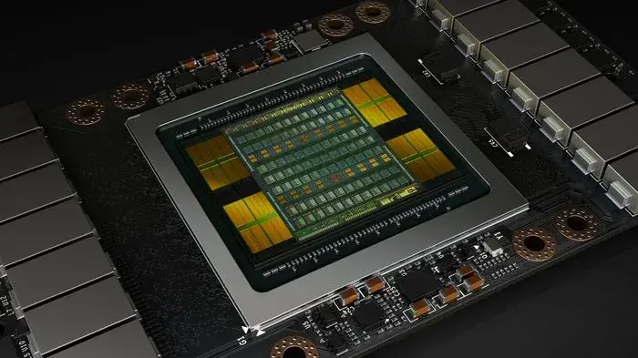
Volta HBM2 accelerator, the cheapest genuine HBM part here and the deepest depreciation curve
NVIDIA V100 is one of 24 data center GPUs tracked in the SecondWatt catalogue, each with specifications, lead times and indicative secondary-market pricing.
NVIDIA V100 dossier: 32 GB HBM2 at 250 to 300 W, SXM2 and PCIe Gen3 variants, rack kW, export position and a documented 83 to 91 percent price decline.
The NVIDIA V100 is a Volta accelerator with 640 tensor cores and 5,120 CUDA cores, published in two form factors. The SXM2 module runs 300 W with 32 GB of HBM2 at 900 GB/s and NVLink at 300 GB/s; the PCIe card runs 250 W with 32 GB or 16 GB at 900 GB/s over a PCIe Gen3 interface at 32 GB/s. Compute is 7.8 TFLOPS FP64 and 125 TFLOPS tensor on SXM2, against 7.0 and 112 on PCIe. Two capability limits decide whether this part is usable at all, and neither is visible in a FLOPS number. Volta tensor cores are FP16 only: there is no FP8, no BF16 and no TF32, so a V100 cannot run an FP8-quantised model. And the PCIe interface is Gen3 at 32 GB/s, half the link bandwidth of every other part in this category and an eight-year-old host requirement. What it offers is real HBM bandwidth and genuine double precision at the lowest price in the category. It also carries the deepest documented depreciation curve in this category: a 32 GB part listed at $11,458 in May 2018 against a Q3 2026 broker band of $1,000 to $2,000, which is 83 to 91 percent over 8.33 years or roughly 19 to 25 percent a year. Azure kept V100-based instances in service about 7.5 years before retiring them in September 2025.
Why it matters
This part shows where accelerator depreciation ends. At 83 to 91 percent off its 2018 price the asks have stopped falling, clustering between $625 and $998 across six weeks, which is where exponential decline becomes scrap-value arithmetic. It is also the one part in this category not named in any export control list reviewed, which is a large part of why it still moves.
Who buys it
Teaching, development and legacy scientific computing buyers who need real HBM bandwidth and FP64 at the lowest possible price. Academic clusters and dev environments dominate. The buyer must confirm the workload runs in FP16 or FP32 before purchase, because the absence of FP8, BF16 and TF32 is a hard capability ceiling rather than a performance penalty.
Role in the data center
Legacy scientific computing, teaching and development clusters, and inference where FP16 is sufficient. Genuine FP64 at 7.0 to 7.8 TFLOPS is the reason it survives in academic use. Lands around a 25 to 30 kW rack density band on air, with no cooling-plant implication.
Power envelope
- Per accelerator
- 300 W — Verified: Maximum configurable board power, manufacturer specification. source
- Cooling class
- Air-coolable — Derived: Per-accelerator power below 400 W — standard air-cooled halls.
No published node-level power rating exists for this part, so node, rack and per-MW figures are not stated. Multiplying accelerator watts by an assumed overhead under-provisions a building by roughly 45% against measured systems.
Node figures are published OEM system ratings; rack counts are arithmetic against a stated rack budget and move with your own cooling design. Assumption set version 2026-09-11a.
Key specifications
| Architecture | Volta |
|---|---|
| Tensor cores | 640 |
| CUDA cores | 5,120 |
| SXM2 memory | 32 GB HBM2 |
| SXM2 memory bandwidth | 900 GB/s |
| SXM2 maximum power | 300 W |
| PCIe memory bandwidth | 900 GB/s |
| PCIe maximum power | 250 W |
| PCIe host interface | PCIe Gen3 32 GB/s |
| SXM2 interconnect | NVLink 300 GB/s |
| SXM2 FP64 | 7.8 TFLOPS |
| PCIe FP64 | 7.0 TFLOPS |
| FP8, BF16 and TF32 support | None |
| Accelerator-only load, 8 SXM2 modules | 2.4 kW |
| Broker band, 32 GB | 1,000 to 2,000 USD, Q3 2026 |
| Named in NVIDIA's 17 October 2023 export filing | No |
Technical summary
Architecture: Volta; 640 tensor cores, 5,120 CUDA cores, ECC memory. SXM2 variant: 32 GB HBM2 at 900 GB/s, 300 W, NVLink at 300 GB/s. PCIe variant: 32 GB or 16 GB HBM2 at 900 GB/s, 250 W, PCIe Gen3 at 32 GB/s. SXM2 compute: FP64 7.8 TFLOPS, FP32 15.7 TFLOPS, tensor 125 TFLOPS. PCIe compute: FP64 7.0 TFLOPS, FP32 14 TFLOPS, tensor 112 TFLOPS. No FP8, no BF16 and no TF32 support; Volta tensor cores are FP16 only. Accelerator-only load, 8 SXM2 modules: 2.4 kW; proxy-estimated node draw, not an OEM figure, 4.9 kW. Observed service life: Azure ran V100 instances about 7.5 years to September 2025. Depreciation: $11,458 in May 2018 to $1,000 to $2,000 in Q3 2026. Not named in NVIDIA's Form 8-K of 17 October 2023 export filing.
Major variations
The two documented variants differ on more than power. V100 SXM2 32GB runs 300 W with 900 GB/s and NVLink at 300 GB/s; V100 PCIe runs 250 W with 900 GB/s over PCIe Gen3 and is offered in 32 GB and 16 GB capacities. FP64 differs too, at 7.8 against 7.0 TFLOPS. Two further NVIDIA designations appear in channel listings and are not confirmed on any current NVIDIA page as of 10 September 2026: V100S PCIe 32GB, reported with higher clocks and 1,134 GB/s at 250 W, and an SXM3 32 GB part rated 350 W used in a second-generation DGX chassis. Treat both as variants to enumerate rather than to specify, and confirm figures with the seller.
Configurations and options
The SXM2 module requires a chassis of its era, a DGX-1 or HGX-1 generation platform, and host availability rather than module availability is the binding constraint. Eight modules at 300 W is 2.4 kW of accelerator load, and NVIDIA's DGX A100 node ratio of 2.03x, used here only as a proxy because the manufacturer publishes no node figure, suggests roughly 4.9 kW. The PCIe card fits any Gen3 or later x16 slot able to cool 250 W. In practice it is deployed in older two-socket servers, four to eight cards a node. There is no multi-instance partitioning on Volta, so a card serves one tenant at a time unless the workload manages sharing itself.
Compatibility and dependencies
The PCIe Gen3 host interface is the defining dependency and it is a ceiling rather than a fault: 32 GB/s of link bandwidth against 64 GB/s on every Ampere and Ada part here, and 128 GB/s on Gen5 parts. A modern Gen5 server gains nothing from this card on the link. The harder limit is capability. Volta tensor cores are FP16 only, with no FP8, no BF16 and no TF32, so an FP8-quantised model will not run at all and current frameworks may refuse the architecture outright. Verify the workload before purchase. On the facility side there is nothing demanding: 250 to 300 W per accelerator lands a node near 4.9 kW and a rack around 25 to 30 kW on air, so plan alongside racks and PDUs only.
Pricing and availability
Trend: falling Microway's V100 price analysis of 8 May 2018 lists the 32 GB parts at $11,458, PCIe and SXM alike, and the 16 GB parts at $10,664. Compute Exchange's Q3 2026 band for V100 32GB is $1,000 to $2,000 with a High supply signal. Over 8.33 years that is 82.5 percent to the $2,000 top, 86.9 percent to a $1,500 midpoint and 91.3 percent to the $1,000 floor, compounding at 18.9, 21.7 and 25.4 percent a year. The floor is visible in ask data: six observations across six weeks in 2026 run $625, $650, $650, $709, $719 and $998 with no trend, so the decline has flattened into scrap-value arithmetic. Azure kept V100 instances in service about 7.5 years before retiring them in September 2025. Lead time, new: Out of production. No manufacturer or authorised-channel route for new stock is published as of 10 September 2026; supply is secondary market only.. Lead time, used or refurbished: Immediate from listing venues, with 92 live listings observed for the 32 GB part on 10 September 2026. Compute Exchange rates supply High.. Warranty, new: Not applicable. This part is out of production and bought used..
Lifecycle and maintenance
Three generations behind the current flagship and built on 2017 silicon. NVIDIA's datasheet, revision r5 of January 2020, remains published, so the part is still documented. Azure retired its V100-powered NCv3 instances in September 2025, roughly 7.5 years after launch, which is the best observed service-life figure available anywhere in this category. At this age the practical maintenance assumption is that thermal interface material needs reworking and that HBM retirement counts, not hours, determine remaining life. Operator depreciation schedules of 4 to 6 years are all well exceeded by this part.
Common failure points
- HBM2 memory stack — Rising correctable ECC counts, then retired rows, then uncorrectable errors and job crashes under memory pressure
- Thermal pad and interface degradation — Clocks decline well below rating at constant load, with die temperature climbing steadily
- Connector and gold-finger corrosion — Intermittent detection, link retraining, or the card failing to enumerate after a chassis move
- PCIe Gen3 host requirement — Not a fault but a ceiling: the link runs at 32 GB/s, half of every other part in this category
- Absence of FP8, BF16 and TF32 — Card works perfectly but will not run a quantised model at all, and modern frameworks may refuse the architecture
- Chassis fans on SXM2 platforms — Rising noise then thermal shutdown on a DGX-1 or HGX-1 era chassis
Inspection checklist
Establish the form factor first: SXM2 is 300 W at 1,134 GB/s, PCIe is 250 W at 900 GB/s, and no channel splits pricing. Driver-reported memory must read 32 GB or 16 GB HBM2 as claimed: the 16 GB card is worth materially less. Stream benchmark bandwidth within 10 percent of the variant figure: 1,134 GB/s for SXM2, 900 GB/s for PCIe. Sustained power draw within 5 percent of rating under full load: 300 W for SXM2, 250 W for PCIe. Core counts must enumerate 640 tensor cores and 5,120 CUDA cores: a low count indicates a re-marked die. HBM2 correctable and uncorrectable ECC counters read before purchase: repeat after a 24-hour soak at full load. Retired-page and row-remap logs pulled: on an eight-year-old part this is the single most important reading. PCIe cards train at Gen3 x16 for 32 GB/s only: a Gen4 reading means the card is not a V100.
Procurement channels
Secondary only, and it is unusually fragmented. Compute Exchange is the one broker publishing a band, at $1,000 to $2,000 with High supply. Beyond that the volume moves through listing venues, with 92 live listings observed for the 32 GB part on 10 September 2026. At this unit value the transaction cost of a formal broker process approaches the value of the part, which is why the channel looks the way it does. Every listing-venue figure captured was an asking price rather than a completed sale.
Regional notes
Appears unrestricted: NVIDIA's Form 8-K of 17 October 2023 does not name it and a July 2026 restrictions compilation does not list it. Neither BIS nor NVIDIA publishes a classification either way, and absence from a filing is not one. BIS guidance of 31 May 2026 turns on the counterparty: a licence is required for any entity headquartered in Country Group D:5 or Macau, or with an ultimate parent there, from every destination outside the US, regardless of location. 91 FR 1684 of 15 January 2026 gates case-by-case China and Macau review at both total processing performance under 21,000 and DRAM bandwidth under 6,500 GB/s. Its 900 to 1,134 GB/s is far under the gate.